
TECHNOLOGY

Smart-GaNᵀᴹ
Gallium Nitride (GaN) power devices switch faster and are more efficient than conventional silicon-based devices. This enables a new generation of power conversion solutions with reduced size, weight, and environmental impact.
Despite the great potential, Driving GaN High Electron Mobility Transistors (GaN HEMTs) presents unique challenges owing to their inherent characteristics, such as fast switching speeds and high input capacitance. The need for precise control and effective handling of these features becomes crucial in optimizing the performance of GaN HEMTs in various applications. Traditional drivers may struggle to provide the necessary slew rates and voltage handling capabilities, leading to suboptimal performance, increased power dissipation, and potential reliability issues.
In response to these challenges, the Smart-GaNTM technology introduced by NovaWave emerges as a superior solution: NW GaN devices can be operated exactly like a conventional Silicon MOSFET, without the need for special gate drivers, driving circuitry, or unique gate voltage clamping mechanisms. Our devices show great gate reliability with an allowed gate swing up to 20 V and a positive Vth of 3 V, which avoids any false turn-on event or the need for negative gate voltage. In addition, the Smart-GaNTM technology introduces several additional integrated features such as lossless current sensing, ESD protection, standby mode, under-voltage lockout, and over-temperature protection. All these features are directly embedded in the device and enable a safer and more efficient operation leading to unprecedented reliability and efficiency.
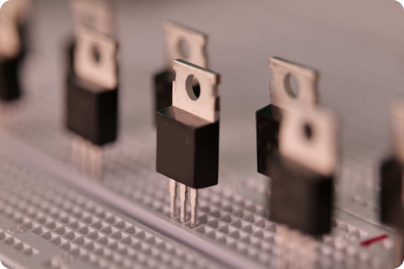
Flash-SBDsᵀᴹ
Schottky Barrier Diodes (SBDs) are fundamental electronic components widely used in power electronics applications such as PFCs and switched power supplies. For a long time, the main solutions on the market were restricted to Si devices, which however exhibit significant limitations.
The material properties of Silicon restrict the use of unipolar (or Schottky) diodes to a range up to 100 V–150 V, with relatively high on-state resistance and leakage current. For higher voltages, p-i-n junctions are employed, which however results in large reverse-recovery behavior and thus are limited to low switching frequencies.
Thanks to the superior properties of wide-bandgap semiconductors, GaN and SiC Schottky diodes can reach a much higher breakdown voltage with low reverse recovery charge and on-resistance. Due to their vertical structure, SiC Schottky diodes are particularly suited for applications in the kV range, especially for industrial and automotive applications, but present some disadvantages in terms of cost and integration for lower voltage ranges < 1 kV, leaving a large market segment unaddressed.
GaN-on-Si SBDs are an ideal solution for applications in the 200 V – 650 V range, resulting in low-cost devices with zero reverse recovery charge, low on-resistance, and low leakage thanks to the unique property of Gallium Nitride grown on a cheap Si substrate. Through our unique technology, NovaWave provides high-performance 650V GaN SBDs at a cost close to silicon solutions but with performance in line with the best silicon carbide devices. With zero reverse recovery and low reverse leakage, our 650 V GaN SBDs series let you take full advantage of the GaN potential and offer a complete GaN portfolio comprising HEMTs, SBDs, and driving ICs.
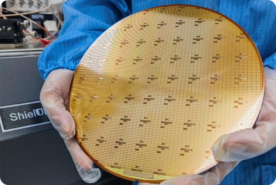
GaN-on-QSTᵀᴹ
GaN epitaxial growth is a key step of the GaN power technology. Currently, GaN-on-Si and GaN-on-sapphire are the most common platforms in the industry, both presenting advantages and drawbacks. GaN-on-sapphire comes from long-term experience in LED and offers a cost-effective solution with a relatively simple buffer structure. However, scalability above 6 inches is still challenging due to uniformity issues, increasing manufacturing cost/die, and the substrate thermal conductivity is low, increasing the device junction-to-case resistance. GaN-on-Si is very attractive from the cost point of view since 8-inch substrates are readily available and wafers can be processed in conventional Si fabs, reducing the cost. Nevertheless, a sophisticated GaN buffer is required, whose thickness is limited to about 5 um by the large lattice mismatch between GaN and Si. This can result in dynamic Ron degradation and limit the maximum voltage rating of the GaN device due to vertical buffer breakdown.
GaN-on-QST successfully addresses these challenges. Being the QST engineered to have the same thermal expansion coefficient as GaN, it enables thick epitaxial layers, improving reliability and addressing voltage ratings above 650 V. In addition, the QST substrate exhibits larger thermal conductance, improving the device’s thermal dissipation and enabling more power at a lower temperature rise. Finally, GaN-on-QST is readily available in an 8-inch substrate, enabling a reduction of the manufacturing cost per die.
Here at NovaWave, we provide cutting-edge GaN-on-QST devices specifically designed to take full advantage of the QST substrate to deliver optimal performance.

SiC SBDs
Silicon Carbide (SiC) is proving to be a game-changer in power electronics for a large variety of applications. As material, SiC, offers several advantages compared to Silicon, enabling drastically improved efficiency, speed, and reliability in power systems.
One of the standout features of SiC is its remarkable ability to operate at higher temperatures compared to traditional silicon-based counterparts. NovaWave’s SiC Schottky Barrier Diodes (SBDs) take full advantage of this characteristic, ensuring optimal performance and reliability even in challenging thermal environments. The higher thermal conductivity of SiC not only allows for efficient heat dissipation but also translates into systems that can handle increased power loads.
Moreover, SiC exhibits significantly lower conduction losses and faster switching speeds, enabling power electronics to operate with enhanced efficiency. The absence of reverse recovery charge allows operation at high switching frequency, paving the way for new applications and topologies. Reduced power losses mean that devices can perform their functions more effectively, improving the efficiency of the overall system.
NovaWave SiC SBDs embrace these advantages to offer efficient solutions for a wide variety of applications including renewable energy, industrial, and mobility.
